Electronics I – Week #5 Lecture 2
VDB Load Line and Q
Point, Other Types of Bias an PNP Transistor
Voltage
Divider Biasing (VBD):
The
voltage divider biasing as discussed previously is the most popular method
of biasing, which refers to universal biasing or base bias that utilizes only
one supply which provides better bias stability. In order for this
configuration to perform good stability, the resistors must be R1||R2 <
0.01RIN. A well design circuit will satisfy this condition. The
voltage divider sees a load resistance of RIN in order for the
voltage divider to appear firm to the base meaning. The 100:1 ratio should be
considered. This translates to R1||R2 < 0.01RIN for a good
design of Voltage Divider Biasing. The concept of NPN biasing is similar to PNP
biasing. If a student understands the biasing NPN transistor, he or she can
apply it to the biasing of a PNP transistor.
The
emitter resistor RE contributes to the stability of the circuit
in case of different value of β from transistor to transistor. Looking
from the base point of the transistor, the RIN = βdc RE.
Substituting
this equation into the previous equation for the RIN, the overall
equation for the firm voltage divider becomes R1||R2 < 0.01 βdc
RE.
VDB
Design Guideline
Before
proceeding with the design, it is important to determine the circuit
requirements or specifications. The circuit is normally biased for VCE to
be at a midpoint value with a specified collector current. Another important
parameter to know before the design is the value of VCC and
βdc for the particular transistor, which is considered in
the design. It is a good practice to start the emitter voltage VE at
10% of the supply voltage. That is VE = 0.1 VCC.
This assumption assists us to find the value of the RE to set
up the specified collector current: RE = VE/IE
Since
the Q point needs to be at about the middle of the dc load line. Approximately
0.5 VCC appears across the collector–emitter terminals. The
rest of 0.4 VCC appears across the collector resistor.
Therefore, RC = 4 RE. After this point the 100:1
rule mentioned above will be considered. It is worth mentioning here that for
stiff voltage divider one can use 10:1 rule: R2 <=0.1 βdc RE.
Other
types of Bias for a NPN Transistor
Some
of the methods used for providing bias for a transistor are:
1. Base Bias or fixed current bias: Because the current and bias
voltage does not remain constant during the operation of the transistor, this
is not considered a popular and a good method. This circuit can be developed by
just adding an emitter resistor to the base bias circuit.
2. Base Bias with emitter feedback: This circuit achieves good
stability of dc operating point against changes in β with the help of
emitter resistor, which causes to raise degeneration. In this circuit the
following equation is used:
VC = VCC –ICRL;
VE = IERE; IC = (VCC –VBE)
/ (RE + RB/β)
3. Base Bias with collector feedback: This method is well known
as collector to base bias or collector feedback bias. It provides a better
stability (see Figure 1).
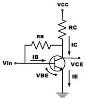
Figure
1
4. Base bias with collector and emitter feedbacks: This method is a
combination of the ii and iii above. This is similar to base bias circuit with
the exception of RB is connected from the base to collector
directly (see Figure 2 below).
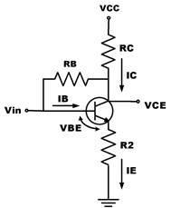
Figure
2
5. Emitter bias with two supplies: This method requires both
a negative power supply and the positive power supply. Unlike the other types,
base in this configuration is connected to the ground (see Figure 3 below).
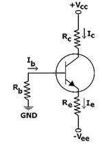
Figure
3
6. Voltage divider bias: This technique, which also can be called a universal
bias circuit, has been discussed in the past lecture (note 5a).
![]()